The Two Dominant PCB Assembly Technologies
Walk through any electronics manufacturing facility and you will see two fundamentally different approaches to attaching components to a printed circuit board. Surface mount technology (SMT) places tiny components directly on pads on the board's surface, while through-hole technology (THT) uses components with wire leads that pass through drilled holes and are soldered on the opposite side. Both methods are mature, well-understood, and actively used in production today — often on the same board.
Choosing correctly between them — or deciding where to use each in a mixed design — requires understanding the mechanical, electrical, cost, and process tradeoffs each technology brings to your product.
Surface Mount Technology (SMT): How It Works
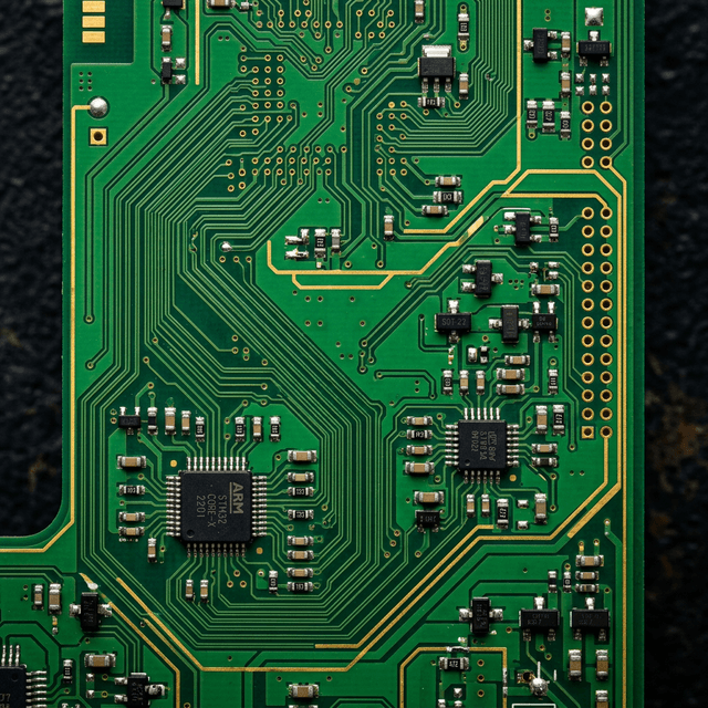
SMT was commercialized in the 1980s and now dominates high-volume electronics manufacturing. In an SMT process, solder paste (a mixture of powdered solder alloy and flux) is stencil-printed onto the board's surface pads. A pick-and-place machine then positions components — chip resistors, capacitors, ICs in QFP, BGA, or LGA packages — onto the paste with high speed and precision. The board then travels through a reflow oven, where controlled temperature profiles melt the paste and form permanent solder joints.
SMT components are specified by standardized package sizes: 0402, 0603, 0805 for passive components; SOT-23, SOIC, QFN, BGA for semiconductors. The smallest production-ready passives (0201 and even 01005) are barely visible to the naked eye, which explains how modern smartphones pack thousands of components into a board the size of a playing card.
Advantages of SMT
- Component density: SMT components are dramatically smaller than their through-hole equivalents. Both sides of the board can be populated, doubling the available real estate.
- Automation: Pick-and-place machines can place tens of thousands of components per hour with placement accuracy measured in microns. Labor cost per joint is low at volume.
- Electrical performance: Shorter lead lengths reduce parasitic inductance and capacitance, which matters for high-frequency designs.
- Cost at volume: Once stencils and programs are created, per-unit cost drops sharply with volume. SMT is cost-efficient for mid- to high-volume production.
Limitations of SMT
- Mechanical strength: SMT solder joints bond to pads on the surface layer only. They can be vulnerable to stress from mechanical shock, vibration, or connector mating forces — particularly for heavier components.
- Rework complexity: Reballing a BGA or removing a fine-pitch QFP requires specialized equipment and skilled technicians.
- Higher NRE for low volumes: Stencils, programming, and setup cost are spread over fewer units at low volumes, making the per-unit economics less favorable for prototypes or small runs.
Through-Hole Technology (THT): How It Works
Through-hole assembly predates SMT. Components have leads — solid wire pins — that are inserted through plated holes drilled in the PCB. Solder is applied either manually with a soldering iron or by passing the populated board over a wave of molten solder (wave soldering). The plated barrel of the hole is filled with solder, creating a joint that mechanically anchors the component through the board's full thickness.
Common through-hole components include electrolytic capacitors, transformers, connectors, relays, large inductors, and certain power semiconductors. Many of these components are available only in through-hole packages because their physical requirements — bulk capacitance, high current, high voltage isolation, or mechanical retention — do not lend themselves to surface-mount packaging.
Advantages of THT
- Mechanical strength: The solder joint extends through the full board thickness. Through-hole connectors and components can withstand repeated mating cycles, vibration, and mechanical stress that would lift SMT pads.
- High-stress applications: Transformers, heavy capacitors, and power modules benefit from the structural support of a through-hole mounting.
- Ease of manual rework: Through-hole joints are accessible and straightforward to desolder and replace with basic equipment.
- High-voltage isolation: The physical separation of through-hole component leads makes it easier to achieve required creepage and clearance distances in high-voltage designs.
Limitations of THT
- Board space: Drilled holes consume routing channels on inner layers. Through-hole pads are much larger than SMT pads. Board size increases.
- Slower assembly: Manual insertion is labor-intensive. Even automated insertion machines are slower than SMT pick-and-place and are only cost-justified for specific component types at volume.
- Single-sided population constraint: Through-hole components must be inserted from one side, limiting component placement flexibility.
Mixed Technology: The Reality of Modern PCB Design
The vast majority of professional PCB designs are mixed-technology boards. A motor controller might use SMT microcontrollers, passives, and MOSFETs for the signal and gate-drive circuitry while using through-hole connectors, large bulk capacitors, and terminal blocks for power connections. An industrial sensor node might be 95% SMT with through-hole mounting holes and a handful of connectors that take mechanical abuse in the field.
Mixed-technology assembly adds process complexity. The typical process flow is:
- Apply solder paste and reflow SMT components on the top side.
- If SMT components exist on the bottom side, apply adhesive and reflow (or wave solder with selective masking).
- Insert through-hole components.
- Wave solder or selectively solder the through-hole joints.
Each additional process step adds cost and the potential for defects. Good design practice minimizes unnecessary complexity: place all SMT components on the top side if possible, keep through-hole components that require wave soldering away from SMT components that cannot tolerate wave temperatures, and consult your CM's DFM guidelines before finalizing the stackup.
When to Use SMT, When to Use THT
Use SMT as your default for:
- Any component available in an SMT package where mechanical stress on the joint will be low.
- High-frequency or RF designs where lead inductance must be minimized.
- High-density boards where board area is constrained.
- Mid- to high-volume production where automation economics favor SMT.
Use through-hole for:
- Connectors that will be mated and unmated repeatedly, or that must resist pull-out forces.
- High-voltage components where creepage and clearance requirements demand physical separation.
- Heavy components (large transformers, bus capacitors) that would stress SMT solder joints under vibration or gravity.
- Components only available in through-hole packages.
- Field-replaceable items where simple rework access matters.
The decision is rarely either/or — it is about placing each component type where its structural and electrical requirements are best met by the available assembly technology.
EMS Technologies
Electronic Manufacturing Insights