
What is Design for Manufacturability and Why Does It Matter?
Design for Manufacturability (DFM) is the practice of designing a PCB so that it can be reliably and cost-effectively manufactured using standard production processes. It is not about compromising electrical performance — it is about ensuring that the choices made in the EDA tool translate cleanly into a manufacturable, testable assembly without unnecessary yield losses, rework, or cost.
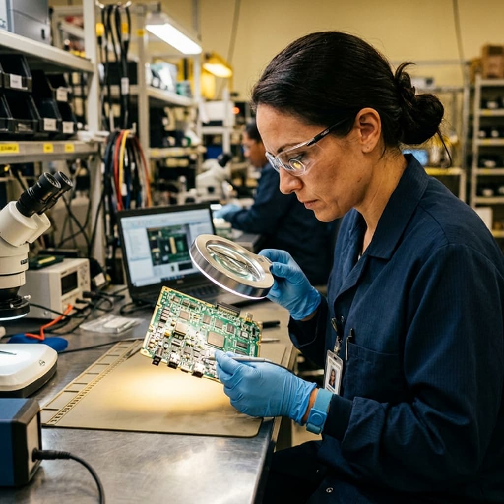
The earlier DFM issues are caught, the cheaper they are to fix. A footprint error found during design review costs minutes to correct. The same error found after bare boards are fabricated costs the entire PCB run. The same error found after populated assemblies fail inspection costs components, labor, and schedule. DFM review before releasing for manufacture is one of the highest-return investments in a hardware development program.
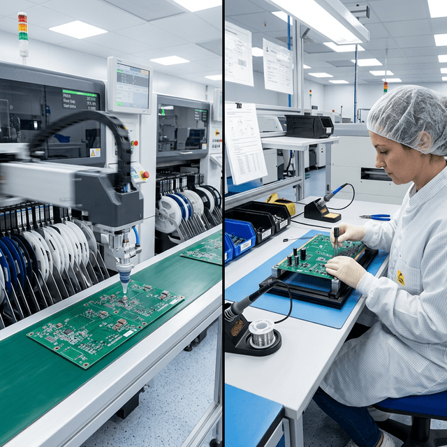
The following checklist covers the most common DFM issues seen in PCB assemblies. It is organized by category and is applicable to the majority of SMT-dominant, mixed-technology boards. Use it before submitting files to your CM — and ask your CM to perform their own DFM review as well, since their process-specific constraints may differ from generic guidelines.
Component Footprints and Placement
1. Courtyard Clearances
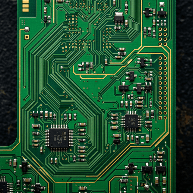
Every component footprint in a well-maintained library includes a courtyard outline that defines the minimum exclusion zone around that component. Verify that no two courtyard outlines overlap. Overlapping courtyards indicate components that cannot be physically placed without conflict — a guaranteed assembly failure. Check this in your EDA tool's design rule check (DRC) before generating Gerbers.
2. Component Orientation Consistency
Align passive components (resistors, capacitors) in consistent orientations — typically horizontal or vertical, with polarity indicators facing a consistent direction. Consistent orientation reduces the visual inspection burden, makes AOI programming more efficient, and reduces the chance of polarity errors on polarized components (electrolytic capacitors, diodes, tantalum caps, ICs).
3. Component-to-Board-Edge Clearance
Maintain a minimum clearance of 5mm (0.2 inches) from any component to the board edge if the board will be depanelized by routing. For v-score panelization, increase this to 3mm minimum and keep tall components (connectors, large capacitors) further away from scored lines, as the scoring and breaking process induces stress. Components too close to the edge can be damaged during depaneling or can interfere with conveyor rails during assembly.
4. Tall Component Placement
Tall components (connectors, electrolytic caps, heat sinks) shadow adjacent components during reflow, creating thermal gradients that can result in cold solder joints. Keep tall components toward the perimeter of the board when possible, and verify clearance for the solder wave if bottom-side through-hole components will be wave soldered.
Fiducials and Registration
5. Global Fiducials
Include at least three global fiducial marks on the board — copper circles (typically 1mm diameter) with a clear copper-free keepout zone (3mm diameter minimum) in the soldermask. Fiducials are used by the pick-and-place machine to register the board position before placing components. Boards without fiducials require the operator to manually define registration points, which increases setup time and reduces placement accuracy. Place fiducials asymmetrically so that the machine can detect if the board is loaded in the wrong orientation.
6. Local Fiducials for Fine-Pitch Components
For QFPs with pitch below 0.5mm, BGAs, or other fine-pitch ICs, add local fiducials adjacent to the component. These allow the pick-and-place machine to fine-correct placement for each individual component rather than relying solely on global registration, improving placement accuracy for components where a few tens of microns of misalignment can cause bridging.
Solder Paste and Stencil
7. Paste Mask Aperture Sizing
Solder paste apertures should be sized to the IPC-7525 stencil design guidelines for your component types. For most SMT components with a standard stencil thickness (0.127mm / 5 mil), the aperture-to-pad area ratio (area ratio) should be above 0.66 to ensure clean paste release from the stencil aperture. If your design includes components with very different paste volume requirements (BGAs alongside 0201s), discuss this with your CM — a step stencil or selective stencil may be appropriate.
8. Thermal Relief on Power Planes
Through-hole pads and large via pads that connect to copper planes should use thermal relief spokes rather than solid connections in most cases. Thermal relief allows the pad to heat up during soldering without the plane acting as a heat sink that prevents the solder from reaching adequate temperature. Solid connections on power plane pads are a common cause of cold solder joints on through-hole components.
Silkscreen and Marking
9. Silkscreen Legibility
Keep silkscreen text and reference designators off of solder pads. Silkscreen ink on pads interferes with solder paste adhesion and can contaminate solder joints. Verify that all reference designators are legible (minimum text height 0.8mm for production legibility), that they are oriented consistently, and that they are not obscured by component bodies after assembly.
10. Polarity and Pin 1 Indicators
Clearly mark polarity on all polarized components (diodes, electrolytic capacitors, tantalum capacitors) and Pin 1 on all ICs. The silkscreen marking should remain visible after the component is installed — do not place the polarity mark under the component body. Use both a silkscreen indicator and a pad shape convention (e.g., square pad for Pin 1) for redundancy.
Test Points
11. Exposed Test Points for Key Nets
Include dedicated test points on critical power rails, control signals, clock lines, and any net that will need to be probed during functional test or debug. Test points should be accessible from one side of the board (top side preferred), sized for the test method planned (minimum 0.9mm for flying probe, larger pads for bed-of-nails fixture pins), and placed in the centroid file so they appear in the pick-and-place data. Designs without test points are significantly harder and more expensive to debug and test.
Component Availability
12. Verify Component Availability Before Releasing
Cross-check every part in your BOM against live distributor inventory before releasing for manufacture. Components with zero stock at all major distributors, end-of-life notices, or lead times longer than your production schedule are BOM risks that will halt your program. For critical components, identify at least one approved alternate part and document it on the BOM.
Panelization
13. Panel Design for Efficient Assembly
For small or irregularly shaped boards, panelization (arranging multiple boards in a larger panel) improves assembly efficiency and reduces per-unit cost. Common methods are v-scoring (a score line that allows snap separation after assembly) and tab routing (boards connected by small tabs that are broken or routed after assembly). Confirm your CM's preferred panelization method and rail requirements (typically 5-10mm border rails with fiducials and tooling holes) before designing your panel.
The Value of CM-Based DFM Review
Even if you work through this entire checklist meticulously, your CM's DFM review is still valuable. Each CM has specific equipment with specific constraints — minimum stencil aperture sizes compatible with their stencil vendor, component height limits for their conveyor system, maximum board sizes for their reflow ovens. A good CM will review your Gerbers and BOM before committing to produce and will flag any process-specific issues the generic checklist does not cover.
Budget time in your program schedule for a DFM review cycle before cutting stencils and ordering components. The few days it adds to the front end of your program will typically pay for themselves many times over in avoided rework, better first-pass yield, and faster time to a clean build.
EMS Technologies
Electronic Manufacturing Insights